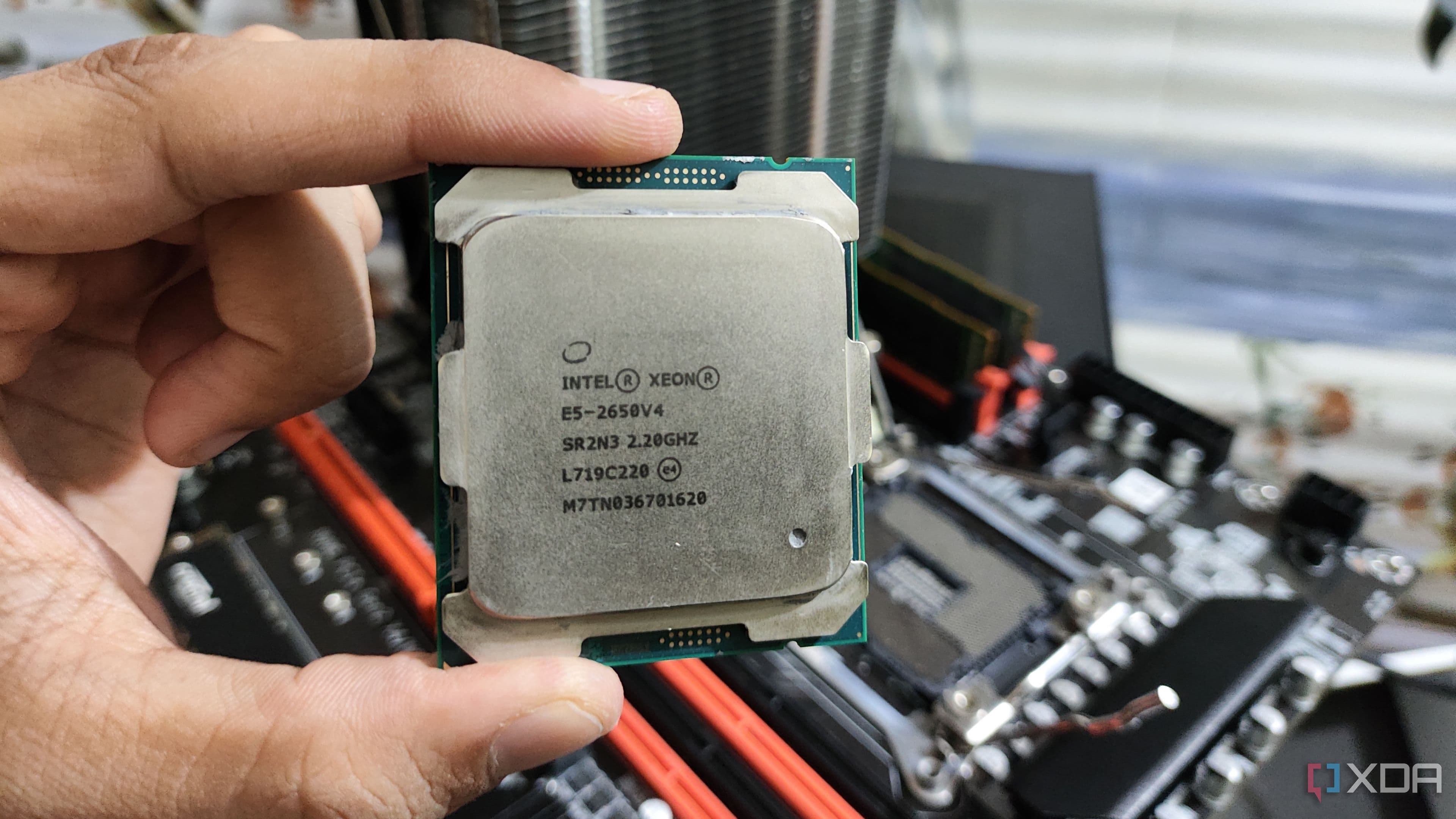
Following experiments that began in 2024, Intel has begun to use ASML's next-generation high numerical aperture (High NA) extreme ultraviolet (EUV) machines, which print circuit patterns on to microchips, to help produce a portion of its Panther Lake processors, ASML said.
Key Insights
10 editorial insights.
Intel has initiated the use of ASML's groundbreaking high numerical aperture (High NA) extreme ultraviolet (EUV) lithography machines to enhance the production of its Panther Lake processors. This development, which began in 2024, marks a significant milestone in semiconductor manufacturing, particularly in the competitive laptop market.
The transition to ASML's High NA EUV technology allows for finer circuit patterns on microchips, enhancing the performance and efficiency of chips. This technology operates at a higher resolution than previous generations, crucial for producing smaller, more powerful transistors. By enabling denser packing of these transistors, Intel aims to deliver improved processing capabilities essential for modern computing tasks.
In the broader context of the semiconductor industry, Intel's adoption of High NA EUV technology places it in a competitive position against rivals like TSMC and Samsung, both of whom are also investing heavily in advanced manufacturing processes. The global demand for high-performance chips continues to surge, with data suggesting that the laptop market alone is expected to grow significantly, driven by remote work and education.
For India, Intel's advancements could catalyze growth in local semiconductor manufacturing and allied tech industries. Indian tech companies, particularly in the hardware and software sectors, may benefit from improved access to advanced chip technologies. Moreover, as India seeks to bolster its semiconductor ecosystem, this development reinforces the nation's strategy to become a key player in global tech supply chains.
Key Highlights
- Intel has begun utilizing ASML's High NA EUV machines for chip production.
- The High NA EUV technology allows for finer circuit patterns on microchips.
- Intel's move is part of a broader trend, with the semiconductor market projected to grow by 20% in the coming years.
- Companies in India’s tech ecosystem stand to gain from these advancements, especially in semiconductor manufacturing.
- Next, we can expect Intel to ramp up production capabilities with the new technology through 2025.
Real-World Impact
Starting now, roles in semiconductor design and manufacturing in India may see increased demand as Intel expands its production capabilities. This includes engineers, quality assurance professionals, and hardware developers. The ripple effects could enhance job opportunities in tech startups focusing on semiconductor innovations and related software developments.
Why This Matters
This shift to advanced EUV technology signifies a pivotal moment for the semiconductor landscape, showcasing a trend toward miniaturization and higher performance. CTOs and developers should consider adapting their strategies to leverage these advanced chips, ensuring their products remain competitive in an evolving market.
Looking ahead, the semiconductor industry will be closely watching Intel's integration of this technology, particularly as it influences chip performance and availability. The upcoming years may bring further advancements that could reshape the market dynamics.
Deep Analysis
Multi-Source Intelligence
Found this useful? Share it!